The ground point in a circuit should be able to BOTH source AND sink currents. The V/2 potential provided by an R+R resistor divider across a V-0 potential is simply that: its a potential. It is able to source current from +V into the circuit through the upper R. But can't sink any. Think about the impedance looking back into the R+R divider from the load circuits' perspective. Usually R+R must be kept very large to minimize idle current consumption.
A real 'ACTIVE' ground is needed for a dual supply opamp. Here is an article that gives you TEN best ways to do it.
(Added Jan 30, 2017Here's an excellent hands-on how-to guide: Tim Williams' Circuit Designer's Companion There are also a couple of other books on the Secrets of good RF analog design by Behzad Razavi in the Central Library
(Added December 27, 2016What causes it? How to fix it
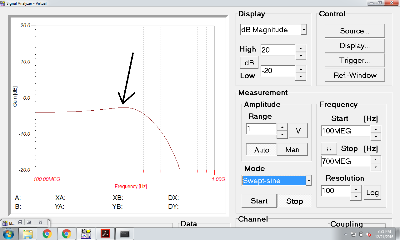
This Bode plot
(sent in by Shobhana for a circuit built around the OPA615) seems to indicate a classic case of gain peaking around the bandwidth pole of the OPA615 (440 MHz).
Sometime you get a slight peak near the first corner frequency. This is called Gain peaking. It will cause your circuit to spontaneously break out into oscillations at the corner frequency. It is almost always some capacitance that is the culprit in opamp feedback circuit. The sharper the peaking, the higher the Q factor associated with such resonant oscillations.
Here are some tips on how to do stability analysis and isolate such problems:
Build a TRANSCONDUCTANCE amplifier. Note that this is the INVERSE of a transimpedance amplifier. Texas Instruments makes a few such IC's : Product List
Note the cost! It's probably a good idea to prototype with the cheaper low bandwidth part. The low bw parts have a different pin config, but that's OK - PCB redesign and printing is cheap! Building a circuit around such high performance IC's is not easy! Always look for the manufacturer's recommended test fixture which will give the recommended board layout of the IC along with associated passive components. OPA615 board layout is hereGenerally we use FR4 PCB substrate material (because it's cheap!) However, for high frequency applications, dielectric constant of the substrate becomes a very important parameter. A different hf-specific substrate called Rogers is used. Here's a document explaining substrate matters.